becomes
infrastructure.
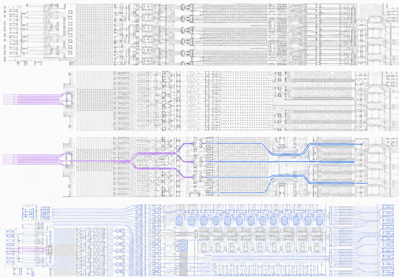
Electrical I/O stopped scaling. Models didn't.
Every hop in today's AI cluster pays for electrical signaling: serialize, drive copper, deserialize, repeat. Above 200G per lane, the energy and area cost of electrical signaling grows faster than the bandwidth it delivers. Co-packaged optics removes the conversion entirely — data leaves the compute die as light.
Three parts. One optical fabric.
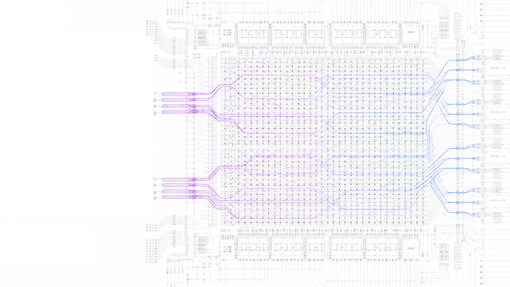
A training processor, a photonic switch, and an inference engine — designed together so light never has to become electricity between them.
Train through the bandwidth wall.
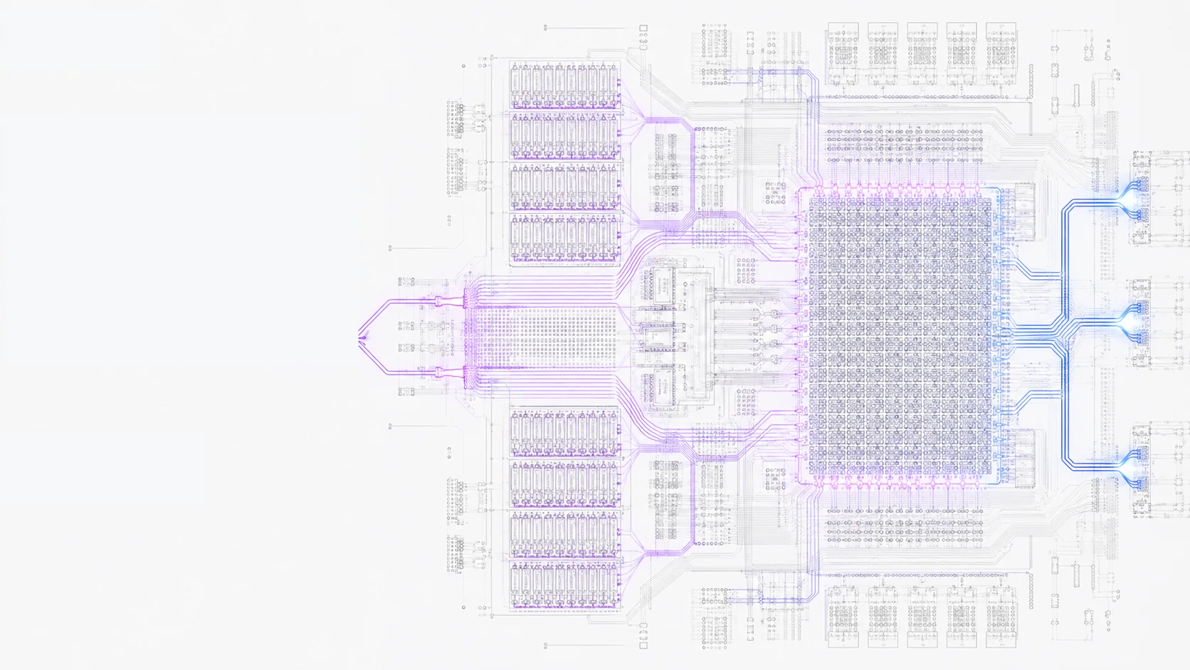
A systolic array fed directly by optics — activations and gradients leave the die as light, and training domains span racks without an electrical hop.
Route in light.
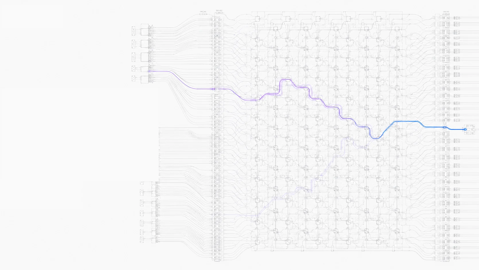
A photonic crossbar between pods. Wavelengths are switched in the optical domain — under a microsecond end to end, no top-of-rack layer at all.
Inference at optical scale.
4–5× lower power per token. Co-packaged HBM holds the KV cache next to the compute; light carries everything that has to travel.
From package to pod without leaving the optical domain.
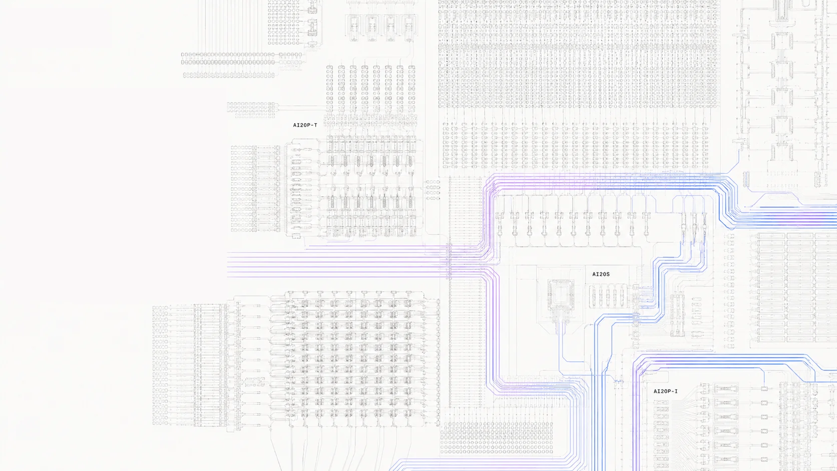
Inside the package, HBM and CMEM SRAM keep data next to the systolic array. Between packages, fibers carry it across the node. Between nodes, the AI20S switch routes it — a flat optical fabric with no top-of-rack layer.
AI20P-T VS COMPETITION

The fabric is light.
Three parts, designed as one.
AI20P-T trains, AI20S routes, AI20P-I serves — and light never has to become electricity between them.
Open the node.
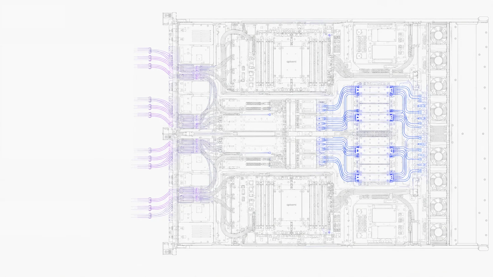
No electrical switch plane.
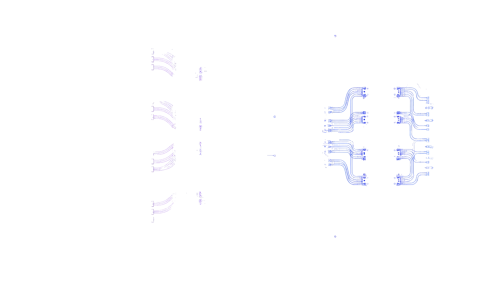
Fibers run from every package straight to the optical fabric — the schematic is the wiring diagram.
From schematic to steel.
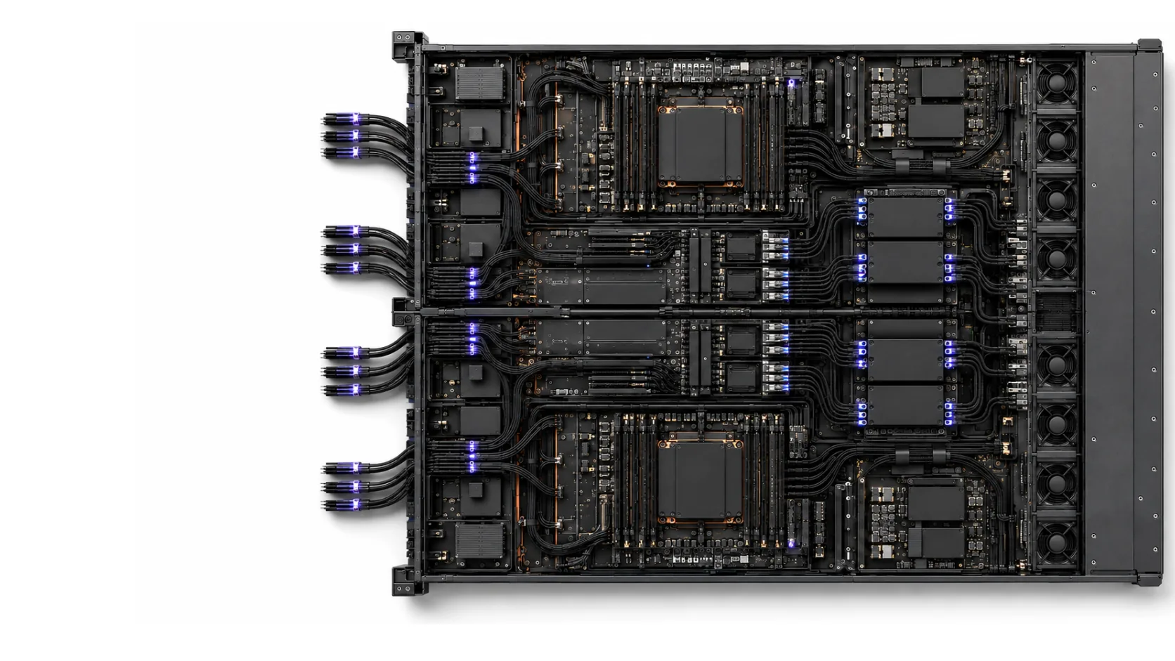
The same node, built: packages, fiber bundles and fans in a standard rack unit.
One node. Then ten thousand.
A 3D torus of light.
Every rack connects to the optical fabric directly — no top-of-rack switches, no oversubscription, no cable clutter.
The fabric doesn't care about distance.
In glass, ten metres costs the same as ten millimetres. The training domain is the whole floor — sub-microsecond, end to end.
Where light goes next.
Photons carry no charge — radiation doesn't flip them. Low power means less radiator mass per FLOP. The same fabric that scales a datacenter floor is built for orbit.
Light becomes infrastructure.
We work with foundries, hyperscalers and systems partners on co-packaged optics, photonic switching and optical compute. If that's your problem space, talk to us.